Difference between revisions of "Config TIAO Universal JTAG Cable As A Buffered Xilinx Parallel Platform Cable III"

10 PCS, 10cm x 10cm, 2 layers prototype for $38.80 shipped!
(New page: <meta name="keywords" content="TIAOWIKI,JTAG,TJTAG,FTA,JTAG,WRT54G,DD-WRT,urjtag, openocd, flashrom,USB jtag, debrick,tomato,router,wireless router,motorola modem,sb5100,wiggler,arm,mips,a...) |
(→Overview) |
||
| (9 intermediate revisions by the same user not shown) | |||
| Line 18: | Line 18: | ||
In this tutorial, I am going to show you how to config it as a Xilinx Buffered Parallel Cable III to erase/read and program Xilinx CPLD. | In this tutorial, I am going to show you how to config it as a Xilinx Buffered Parallel Cable III to erase/read and program Xilinx CPLD. | ||
| + | '''If you have [http://www.diygadget.com/jtag-cables/universal-jtag-adapter-v2-wiggler-and-xilinx-platform-cable-compatible-debrick-routers-modems-and-more.html V2] of our Universal JTAG Adapter, this step is not required as the V2 has onboard pins, all you have to do is to short pins using jumpers.''' | ||
| + | |||
| + | <font color=red>This tutorial works for CPLDs operating on +3.3v voltage only</font> | ||
== Required Hardware == | == Required Hardware == | ||
| Line 23: | Line 26: | ||
* [http://www.diygadget.com/jtag-cables/universal-jtag-adapter-for-routers-modem-fta-and-more.html TIAO Universal Buffered Parallel JTAG Adapter] | * [http://www.diygadget.com/jtag-cables/universal-jtag-adapter-for-routers-modem-fta-and-more.html TIAO Universal Buffered Parallel JTAG Adapter] | ||
| + | [http://www.diygadget.com/jtag-cables/universal-jtag-adapter-for-routers-modem-fta-and-more.html http://www.diygadget.com/media/catalog/product/u/n/universal.jtag.600_2.jpg] | ||
== Xilinx Buffered Platform Cable III Schematic == | == Xilinx Buffered Platform Cable III Schematic == | ||
This is the schematic of the official Xilinx Buffered Platform Cable III: | This is the schematic of the official Xilinx Buffered Platform Cable III: | ||
| + | [[Image:Xilinx.platform.cable3.jpg|none|thumb]] | ||
| − | The | + | The key points of the schematic are as follows: |
| − | |||
| − | |||
| − | |||
| − | |||
| − | |||
| − | |||
| − | |||
| − | |||
| − | |||
| − | |||
| − | |||
| − | |||
| − | |||
| − | |||
| − | |||
| − | |||
| − | |||
| − | |||
| − | |||
| − | |||
| − | |||
| − | |||
| − | |||
| − | |||
| − | |||
| − | |||
| − | |||
| − | |||
| − | |||
| − | |||
| − | |||
| − | |||
| − | |||
| − | |||
| − | |||
| − | |||
| − | |||
| − | |||
| − | |||
| − | |||
| − | |||
| − | |||
| − | |||
| − | |||
| − | |||
| − | |||
| − | |||
| − | |||
| − | |||
| − | |||
| − | |||
| − | |||
| − | |||
| − | |||
| − | |||
| − | |||
| − | |||
| − | |||
| − | |||
| − | |||
| − | |||
| − | |||
| − | |||
| − | |||
| − | |||
| − | |||
| − | |||
| − | |||
| − | |||
| − | |||
| − | |||
| − | |||
| − | |||
| − | |||
| − | |||
| − | |||
| − | |||
| − | |||
| − | |||
| − | |||
| − | |||
| − | |||
| − | |||
| − | |||
| − | |||
| − | |||
| − | |||
| − | + | * PIN 2 of DB25 is TDI | |
| + | * PIN 3 of DB25 is TCK | ||
| + | * PIN 4 of DB25 is TMS | ||
| + | * PIN 13 of DB25 is TDO | ||
| + | * PIN 8, 11 and 12 of DB25 are shorted (connected) | ||
| − | + | Thus, we can simulate the above schematic on TIAO Universal Buffered Parallel JTAG Adapter. | |
| − | + | == Xilinx Buffered Platform Cable III Connections on TIAO Universal Buffered Parallel JTAG Adapter == | |
| − | + | [[Image:Xilinx.on.ujtag-1.jpg|none|thumb]] | |
| − | + | Basically, make the following connections: | |
| − | |||
| − | |||
| − | |||
| − | |||
<pre> | <pre> | ||
| − | + | * Short DB25's pin 8, 11 and 12 | |
| − | + | * Use female to female jumper wire to connect D2, D3, D4, D13 to A1, A2, A3, Y8 on TIAO Universal JTAG adapter respectively. | |
| − | + | * Use female to female jumper wire to connect Y1, Y2, Y3, A8, GND, 3.3V to CPLD's TDI, TCK, TMS, TDO, GND and Vcc respectively. | |
| − | |||
| − | |||
| − | |||
| − | |||
| − | |||
| − | |||
| − | |||
| − | |||
| − | |||
| − | |||
| − | |||
| − | |||
| − | |||
| − | |||
| − | |||
| − | |||
| − | |||
| − | |||
| − | |||
| − | |||
| − | |||
| − | |||
| − | |||
| − | |||
| − | |||
| − | |||
| − | |||
| − | |||
| − | |||
| − | |||
| − | |||
| − | |||
| − | |||
| − | |||
| − | |||
| − | |||
| − | |||
| − | |||
| − | |||
| − | |||
| − | |||
| − | |||
| − | |||
| − | |||
| − | |||
| − | |||
| − | |||
| − | |||
| − | |||
| − | |||
| − | |||
| − | |||
| − | |||
| − | |||
| − | |||
| − | |||
| − | |||
| − | |||
| − | |||
| − | |||
| − | |||
| − | |||
| − | |||
| − | |||
| − | |||
| − | |||
| − | |||
| − | |||
| − | |||
| − | |||
| − | |||
| − | |||
| − | |||
| − | |||
| − | |||
| − | |||
| − | |||
| − | |||
| − | |||
| − | |||
| − | |||
| − | |||
| − | |||
| − | |||
| − | |||
| − | |||
| − | |||
| − | |||
| − | |||
| − | |||
| − | |||
| − | |||
| − | |||
| − | |||
| − | |||
| − | |||
</pre> | </pre> | ||
| − | + | == Short DB25's PIN 8, 11 and 12 == | |
| − | |||
| − | |||
| − | |||
| − | |||
| − | |||
| − | |||
| − | |||
| − | |||
| − | |||
| − | + | In this step, you need to solder wires to make DB25's PIN 8, 11 and 12 connected. | |
| − | |||
| − | |||
| + | [[Image:Xilinx.81112.jpg|none|thumb]] | ||
| − | + | I soldered them together with a leg of a resistor: | |
| − | + | [[Image:xilinx.81112-1.jpg|none|thumb]] | |
| − | |||
| − | + | == Connect the female to female wires == | |
| − | + | In this example, I use XC2C64A CoolRunner-II CPLD Dev Board (RGH) as the example: | |
| − | + | [[Image:xilinx.first.jpg|none|thumb]] | |
| − | + | [[Image:xilinx.2.jpg|none|thumb]] | |
| − | |||
| − | + | [[Image:Xilinx.3.jpg|none|thumb]] | |
| − | |||
| − | |||
| − | |||
| − | |||
| − | |||
| − | |||
| − | |||
| − | |||
| − | |||
| − | |||
| − | |||
| − | |||
| − | |||
| − | |||
| − | |||
| − | |||
| − | |||
| − | |||
| − | |||
| − | |||
| − | |||
| − | |||
| − | |||
| − | |||
| − | |||
| − | |||
| − | |||
| − | |||
| − | |||
| − | |||
| − | |||
| − | |||
| − | |||
| − | |||
| − | |||
| − | |||
| − | |||
| − | |||
| − | |||
| − | |||
| − | |||
| − | |||
| − | |||
| − | [[Image: | ||
| − | |||
| − | |||
| − | |||
| − | |||
| − | |||
| − | |||
| − | |||
| − | |||
| − | |||
| − | |||
| − | |||
| − | |||
| − | |||
| − | |||
| − | |||
| − | |||
| − | |||
| − | |||
| − | |||
| + | == Connect the JTAG board to PC == | ||
| − | + | * Connect the JTAG board and your PC with a USB A to Mini USB cable (most digital camera supplies this kind of cable) | |
| + | * Plug the board to your PC's parallel port | ||
| + | * Run Xilinx iMPACT from lab tools, select Parallel Cable III in cable setup dialog | ||
| + | * Now, you can use iMPACT to read/erase/write CPLDs. | ||
| + | [[Image:xilinx.4.jpg|none|thumb]] | ||
| + | You can read [[Program Xilinx XC2C64A Or Similar Xilinx CPLD Using TIAO Universal JTAG Cable]] on how to program CPLD using our Universal Parallel JTAG board. | ||
<span class="plainlinks"> | <span class="plainlinks"> | ||
Latest revision as of 03:21, 15 May 2012
Contents
Buy various JTAG cables for your Satellite Receiver, Cable Modem, Wireless Router, Standard Wiggler from http://www.easymg.com and http://www.diygadget.com
Overview
TIAO Universal Buffered Parallel JTAG Adapter is a multi-functional parallel JTAG adapter for hobbyists or engineers.
In this tutorial, I am going to show you how to config it as a Xilinx Buffered Parallel Cable III to erase/read and program Xilinx CPLD. If you have V2 of our Universal JTAG Adapter, this step is not required as the V2 has onboard pins, all you have to do is to short pins using jumpers.
This tutorial works for CPLDs operating on +3.3v voltage only
Required Hardware
Xilinx Buffered Platform Cable III Schematic
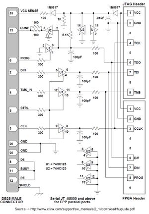
This is the schematic of the official Xilinx Buffered Platform Cable III:
The key points of the schematic are as follows:
- PIN 2 of DB25 is TDI
- PIN 3 of DB25 is TCK
- PIN 4 of DB25 is TMS
- PIN 13 of DB25 is TDO
- PIN 8, 11 and 12 of DB25 are shorted (connected)
Thus, we can simulate the above schematic on TIAO Universal Buffered Parallel JTAG Adapter.
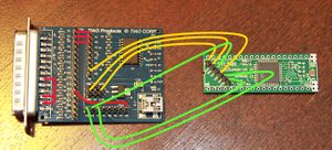
Xilinx Buffered Platform Cable III Connections on TIAO Universal Buffered Parallel JTAG Adapter
Basically, make the following connections:
* Short DB25's pin 8, 11 and 12
* Use female to female jumper wire to connect D2, D3, D4, D13 to A1, A2, A3, Y8 on TIAO Universal JTAG adapter respectively.
* Use female to female jumper wire to connect Y1, Y2, Y3, A8, GND, 3.3V to CPLD's TDI, TCK, TMS, TDO, GND and Vcc respectively.
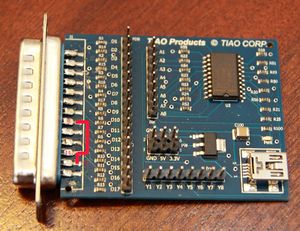
Short DB25's PIN 8, 11 and 12
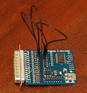
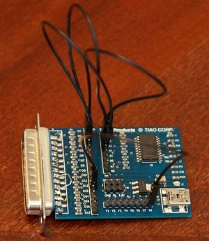
In this step, you need to solder wires to make DB25's PIN 8, 11 and 12 connected.
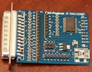
I soldered them together with a leg of a resistor:
Connect the female to female wires
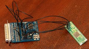
In this example, I use XC2C64A CoolRunner-II CPLD Dev Board (RGH) as the example:
Connect the JTAG board to PC
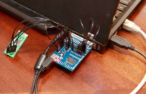
- Connect the JTAG board and your PC with a USB A to Mini USB cable (most digital camera supplies this kind of cable)
- Plug the board to your PC's parallel port
- Run Xilinx iMPACT from lab tools, select Parallel Cable III in cable setup dialog
- Now, you can use iMPACT to read/erase/write CPLDs.
You can read Program Xilinx XC2C64A Or Similar Xilinx CPLD Using TIAO Universal JTAG Cable on how to program CPLD using our Universal Parallel JTAG board.
Buy various JTAG cables for your Satellite Receiver, Cable Modem, Wireless Router, Standard Wiggler from http://www.easymg.com and http://www.diygadget.com

10 PCS, 10cm x 10cm, 2 layers prototype for $38.80 shipped!

