Difference between revisions of "TIAO Black Flash USB+ Universal Flash Programmer User's Manual"

10 PCS, 10cm x 10cm, 2 layers prototype for $38.80 shipped!
| Line 85: | Line 85: | ||
# [[#Reset_Button|Reset Button]] | # [[#Reset_Button|Reset Button]] | ||
# [[#Mode_Change_Switch|Mode Change Switch]] | # [[#Mode_Change_Switch|Mode Change Switch]] | ||
| + | # [[#Flash_Programmer_Pinout|Flash Programmer Pinout]] | ||
= Connector Pinout & LEDs = | = Connector Pinout & LEDs = | ||
| Line 173: | Line 174: | ||
In Application Mode, pressing the reset button will only perform a USB reset. In Bootloader Mode, it will reset the device but when the device automatically reconnects, it will start in the DFU mode, allowing the software to load new AVR firmware. | In Application Mode, pressing the reset button will only perform a USB reset. In Bootloader Mode, it will reset the device but when the device automatically reconnects, it will start in the DFU mode, allowing the software to load new AVR firmware. | ||
| − | == | + | == Flash Programmer Pinout == |
| − | |||
| − | + | The pinout of the flash programmer depends on the firmware loaded into the programmer. | |
| + | [[Image:Pinout-bfu+.png|none]] | ||
| + | |||
| + | '''JTAG Mode Pinout:''' | ||
{| | {| | ||
! align="left"|Pin # | ! align="left"|Pin # | ||
| − | |||
| − | |||
| − | |||
! Description | ! Description | ||
|- | |- | ||
| 1 | | 1 | ||
| − | | | + | | GND |
| − | |||
| − | |||
| − | |||
|- | |- | ||
| 2 | | 2 | ||
| − | | | + | | TCK |
| − | |||
| − | |||
| − | |||
|- | |- | ||
| 3 | | 3 | ||
| − | | | + | | GND |
| − | |||
| − | |||
| − | |||
|- | |- | ||
| 4 | | 4 | ||
| − | | | + | | TMS |
| − | |||
| − | |||
| − | |||
|- | |- | ||
| 5 | | 5 | ||
| − | | | + | | GND |
| − | |||
| − | |||
| − | |||
|- | |- | ||
| 6 | | 6 | ||
| − | | | + | | TDO |
| − | |||
| − | |||
| − | |||
|- | |- | ||
| 7 | | 7 | ||
| − | | | + | | GND |
| − | |||
| − | |||
| − | |||
|- | |- | ||
| 8 | | 8 | ||
| − | | | + | | TDI |
| − | |||
| − | |||
| − | |||
|- | |- | ||
| 9 | | 9 | ||
| − | | | + | | GND |
| − | | | + | |- |
| − | | | + | | 10 |
| − | | | + | | TRST |
|} | |} | ||
| − | + | '''SPI Mode Pinout:''' | |
| − | |||
| − | |||
| − | |||
{| | {| | ||
! align="left"|Pin # | ! align="left"|Pin # | ||
| Line 249: | Line 222: | ||
|- | |- | ||
| 1 | | 1 | ||
| − | |||
| − | |||
| − | |||
| − | |||
| − | |||
| − | |||
| − | |||
| − | |||
| − | |||
| − | |||
| − | |||
| − | |||
| − | |||
| − | |||
| − | |||
| GND | | GND | ||
| − | |||
| − | |||
| − | |||
| − | |||
| − | |||
| − | |||
| − | |||
| − | |||
| − | |||
| − | |||
| − | |||
| − | |||
| − | |||
| − | |||
| − | |||
| − | |||
| − | |||
| − | |||
| − | |||
|- | |- | ||
| 2 | | 2 | ||
| − | | | + | | Vcc |
|- | |- | ||
| 3 | | 3 | ||
| − | | | + | | |
|- | |- | ||
| 4 | | 4 | ||
| − | | | + | | SI |
|- | |- | ||
| 5 | | 5 | ||
| − | | | + | | |
|- | |- | ||
| 6 | | 6 | ||
| − | | | + | | SO |
|- | |- | ||
| 7 | | 7 | ||
| − | | | + | | RST |
|- | |- | ||
| 8 | | 8 | ||
| − | | | + | | SCLK |
|- | |- | ||
| 9 | | 9 | ||
| − | | | + | | PROG |
|- | |- | ||
| 10 | | 10 | ||
| − | | | + | | CS |
|} | |} | ||
| − | + | '''NAND Mode Pinout:''' | |
| − | |||
| − | |||
| − | |||
{| | {| | ||
! align="left"|Pin # | ! align="left"|Pin # | ||
| Line 322: | Line 258: | ||
|- | |- | ||
| 1 | | 1 | ||
| − | |||
| − | |||
| − | |||
| − | |||
| − | |||
| − | |||
| − | |||
| − | |||
| − | |||
| − | |||
| − | |||
| − | |||
| − | |||
| − | |||
| − | |||
| − | |||
| − | |||
| − | |||
| − | |||
| − | |||
| − | |||
| − | |||
| − | |||
| − | |||
| − | |||
| − | |||
| − | |||
| − | |||
| − | |||
| − | |||
| − | |||
| − | |||
| − | |||
| GND | | GND | ||
| − | |||
| − | |||
| − | |||
| − | |||
| − | |||
| − | |||
| − | |||
| − | |||
| − | |||
| − | |||
| − | |||
| − | |||
| − | |||
| − | |||
| − | |||
| − | |||
| − | |||
| − | |||
| − | |||
| − | |||
| − | |||
| − | |||
| − | |||
| − | |||
| − | |||
| − | |||
| − | |||
| − | |||
| − | |||
| − | |||
| − | |||
| − | |||
| − | |||
| − | |||
| − | |||
| − | |||
| − | |||
| − | |||
| − | |||
| − | |||
| − | |||
| − | |||
| − | |||
| − | |||
| − | |||
| − | |||
| − | |||
| − | |||
| − | |||
| − | |||
| − | |||
| − | |||
| − | |||
| − | |||
| − | |||
| − | |||
| − | |||
|- | |- | ||
| 2 | | 2 | ||
| − | | | + | | Vcc |
|- | |- | ||
| 3 | | 3 | ||
| − | | | + | | EJ |
|- | |- | ||
| 4 | | 4 | ||
| − | | | + | | SI |
|- | |- | ||
| 5 | | 5 | ||
| − | | | + | | XX |
|- | |- | ||
| 6 | | 6 | ||
| − | | | + | | SO |
|- | |- | ||
| 7 | | 7 | ||
| − | | | + | | KSK |
|- | |- | ||
| 8 | | 8 | ||
| − | | | + | | SCLK |
|- | |- | ||
| 9 | | 9 | ||
| − | | | + | | |
|- | |- | ||
| 10 | | 10 | ||
| − | |||
| − | |||
| − | |||
| − | |||
| − | |||
| − | |||
| − | |||
| − | |||
| − | |||
| − | |||
| − | |||
| − | |||
| − | |||
| − | |||
| − | |||
| − | |||
| − | |||
| − | |||
| − | |||
| − | |||
| − | |||
| − | |||
| − | |||
| − | |||
| − | |||
| − | |||
| − | |||
| − | |||
| − | |||
| − | |||
| CS | | CS | ||
| − | |||
| − | |||
| − | |||
|} | |} | ||
| + | For detailed firmware/pinout configuration, please read the flashcatUSB software manual downloaded from [http://www.tiaowiki.com/download//file.php?id=39 here]. | ||
| − | |||
| − | |||
| − | |||
| − | |||
| − | |||
| − | |||
| − | |||
| − | |||
| − | |||
| − | |||
| − | |||
| − | |||
| − | |||
| − | |||
| − | |||
| − | |||
| − | |||
| − | |||
| − | |||
| − | |||
| − | |||
| − | |||
| − | |||
| − | |||
| − | |||
| − | |||
| − | |||
| − | |||
| − | |||
| − | |||
| − | |||
| − | |||
| − | |||
| − | |||
| − | |||
| − | |||
| − | |||
| − | |||
| − | |||
| − | |||
| − | |||
| − | |||
| − | |||
| − | |||
| − | |||
| − | |||
| − | |||
| − | |||
| − | |||
| − | |||
| − | |||
| − | |||
| − | |||
| − | |||
| − | |||
| − | |||
| − | |||
| − | |||
| − | |||
| − | |||
| − | |||
| − | |||
| − | |||
| − | |||
| − | |||
| − | |||
| − | |||
| − | |||
| − | |||
| − | |||
| − | |||
| − | |||
| − | |||
| − | |||
| − | |||
| − | |||
| − | |||
| − | |||
| − | |||
| − | |||
| − | |||
| − | |||
| − | |||
| − | |||
| − | |||
| − | |||
| − | |||
| − | |||
| − | |||
| − | |||
| − | |||
| − | |||
| − | |||
| − | |||
| − | |||
| − | |||
| − | |||
| − | |||
| − | |||
| − | |||
| − | |||
| − | |||
| − | |||
<span class="plainlinks"> | <span class="plainlinks"> | ||
Revision as of 21:05, 2 September 2013
Contents
Buy various JTAG cables for your Satellite Receiver, Cable Modem, Wireless Router, Standard Wiggler from http://www.easymg.com and http://www.diygadget.com
Overview
The TIAO Black Flash USB+ Universal Flash Programmer (BlackflashUSB+) is a universal flash programmer with integrated USB to Serial converter (TTL level) and 2 port USB 2.0 hub. It is fully compatible with flashcatusb, thus you can use open source software to program your flash chips.
Technical Specifications
USB 2.0 Hub:
- Compliant to USB specification Revision 2.0
- Integrate USB 2.0 transceiver
- Support 4/3/2 downstream ports by I/O pin configuration
- Upstream port supports both high-speed (HS) and full-speed (FS) traffic
- Downstream ports support HS, FS, and low-speed (LS) traffic
- 1 control pipe (endpoint 0, 64-byte data payload) and 1 interrupt pipe (endpoint 1, 1-byte data payload)
- Backward compatible to USB specification Revision 1.1
- On-chip 8-bit micro-processor
USB to Serial Transceiver:
- Fully Compliant with USB Specification v2.0 (Full-Speed)
- Supports RS232-like Serial Interface
- Full-duplex transmitter and receiver (TXD and RXD)
- Six MODEM control pins (RTS, CTS, DTR, DSR, DCD, and RI)
- 5, 6, 7 or 8 data bits
- Odd, Even, Mark, Space, or None parity mode
- One, one and a half, or two stop bits
- Parity error, frame error, and serial break detection
- Programmable baud rate from 75 bps to 6 Mbps
- External RS232 driver power down control
- Independent power source for serial interface
- Extensive Flow Control Mechanism
- Adjustable high/low watermark level
- Automatic flow control with CTS/RTS
- Automatic flow control with XON/XOFF
- Inbound data buffer overflow detection
- Configurable 512-byte bi-directional data buffer
- 256-byte outbound buffer and 256-byte inbound buffer; or 128-byte outbound buffer and 384-byte inbound buffer
- Supports remote wake-up from MODEM input signals
- Provides drivers support for Windows, Mac OS, Linux, and WinCE
- Designed for Windows XP Certified Logo Drivers
Flash Chip Programmer:
- Open-source software supports multi-languages: English, French, German, Portuguese, Spanish
- Fast 16MHz RISC processor
- 32KB Flash
- Two (2) DIP switches for mode application changes
- Upgradeable firmware over USB
- On board reset button
- Universal CFI Flash programming support
- SPI Mode 0, 1, 2 compatible
- USB 1.1 / 2.0 compatible
- Dual voltage (3.3v or 5v) output
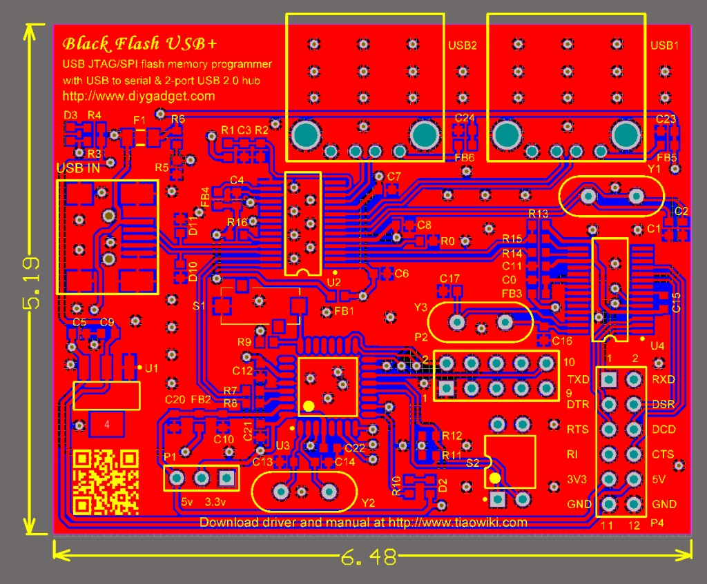
Board Dimensions
The dimension of the board is 6.48 cm * 5.19 cm.
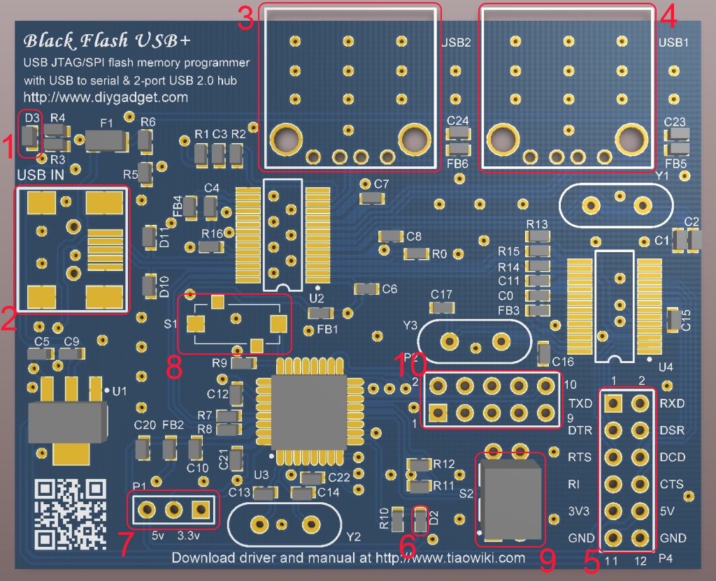
Board Layout
- USB 2.0 Hub power LED
- Mini USB receptacle
- Onboard USB 2.0 port 2
- Onboard USB 2.0 port 1
- Serial (TTL Level) header
- Application Status LED Indicator
- Output Voltage Selector
- Reset Button
- Mode Change Switch
- Flash Programmer Pinout
Connector Pinout & LEDs
USB 2.0 Hub power LED
This LED indicates the onboard USB 2.0 hub is working correctly.
Mini USB receptacle
Connect this receptacle to the computer with a good quality USB to Mini USB cable. The shorter the better.
Onboard USB 2.0 port 2
USB A 2.0 receptacle for any USB 2.0 devices.
Onboard USB 2.0 port 1
USB A 2.0 receptacle for any USB 2.0 devices.
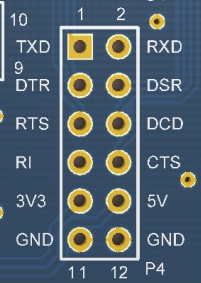
Serial (TTL Level) header
The TTL level COM port header.
| Pin # | Description |
|---|---|
| 1 | Tx |
| 2 | Rx |
| 3 | DTR |
| 4 | DSR |
| 5 | RTS |
| 6 | DCD |
| 7 | RI |
| 8 | CTS |
| 9 | +3.3V |
| 10 | +5V (USB Power) |
| 11, 12 | GND |
Application Status LED Indicator
Indicates the current application status of the flash programmer.
Output Voltage Selector
Move the jumper to 3.3V if the target device support 3.3v. Move the jumper to 5v if the target device supports 5v.
Reset Button
Resets the device or force the programmer to enter the bootloader mode.
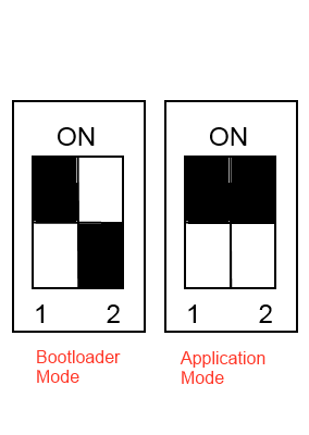
Mode Change Switch
Application mode change switch.
The functionality of this programmer differs depending on the type of firmware programmed into it.
Change to bootloader mode (1 at ON position, 2 away from ON position) (also known as the DFU mode) to perform a firmware update over USB.
Change to application mode (both 1 and 2 at ON position) to execute the firmware loaded into the programmer.
In Application Mode, pressing the reset button will only perform a USB reset. In Bootloader Mode, it will reset the device but when the device automatically reconnects, it will start in the DFU mode, allowing the software to load new AVR firmware.
Flash Programmer Pinout
The pinout of the flash programmer depends on the firmware loaded into the programmer.
JTAG Mode Pinout:
| Pin # | Description |
|---|---|
| 1 | GND |
| 2 | TCK |
| 3 | GND |
| 4 | TMS |
| 5 | GND |
| 6 | TDO |
| 7 | GND |
| 8 | TDI |
| 9 | GND |
| 10 | TRST |
SPI Mode Pinout:
| Pin # | Description |
|---|---|
| 1 | GND |
| 2 | Vcc |
| 3 | |
| 4 | SI |
| 5 | |
| 6 | SO |
| 7 | RST |
| 8 | SCLK |
| 9 | PROG |
| 10 | CS |
NAND Mode Pinout:
| Pin # | Description |
|---|---|
| 1 | GND |
| 2 | Vcc |
| 3 | EJ |
| 4 | SI |
| 5 | XX |
| 6 | SO |
| 7 | KSK |
| 8 | SCLK |
| 9 | |
| 10 | CS |
For detailed firmware/pinout configuration, please read the flashcatUSB software manual downloaded from here.
Buy various JTAG cables for your Satellite Receiver, Cable Modem, Wireless Router, Standard Wiggler from http://www.easymg.com and http://www.diygadget.com

10 PCS, 10cm x 10cm, 2 layers prototype for $38.80 shipped!


