TIAO Black Flash USB+ Universal Flash Programmer User's Manual

10 PCS, 10cm x 10cm, 2 layers prototype for $38.80 shipped!
Contents
- 1 Overview
- 2 Technical Specifications
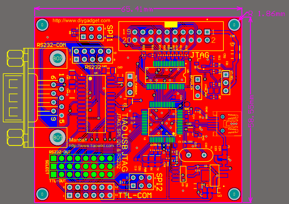
- 3 Board Dimensions
- 4 Board Layout
- 5 Connector Pinout & LEDs
- 5.1 DB9 Male RS232
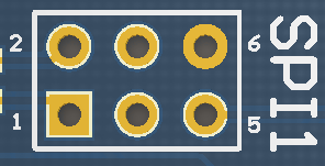
- 5.2 SPI Connector 1
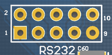
- 5.3 RS232 Level 2.54mm IDC Header
- 5.4 20 PIN JTAG Connector
- 5.5 MAX3243 Auto Power Down Jumper
- 5.6 Buffer Enable Jumper
- 5.7 Buffer Chip Power Selection Jumper
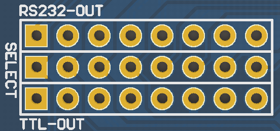
- 5.8 Serial RS232/TTL level Selection Jumper
- 5.9 TTL Level Serial Connector
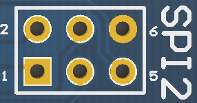
- 5.10 SPI Connector 2
- 5.11 PWR/RX/TX LEDs
- 5.12 Target Board Power LED
- 6 Pin Connections
Buy various JTAG cables for your Satellite Receiver, Cable Modem, Wireless Router, Standard Wiggler from http://www.easymg.com and http://www.diygadget.com
Overview
The TIAO Black Flash USB+ Universal Flash Programmer (BlackflashUSB+) is a universal flash programmer with integrated USB to Serial converter (TTL level) and 2 port USB 2.0 hub. It is fully compatible with flashcatusb, thus you can use open source software to program your flash chips.
Technical Specifications
USB 2.0 Hub:
- Compliant to USB specification Revision 2.0
- Integrate USB 2.0 transceiver
- Support 4/3/2 downstream ports by I/O pin configuration
- Upstream port supports both high-speed (HS) and full-speed (FS) traffic
- Downstream ports support HS, FS, and low-speed (LS) traffic
- 1 control pipe (endpoint 0, 64-byte data payload) and 1 interrupt pipe (endpoint 1, 1-byte data payload)
- Backward compatible to USB specification Revision 1.1
- On-chip 8-bit micro-processor
USB to Serial Transceiver:
- Fully Compliant with USB Specification v2.0 (Full-Speed)
- Supports RS232-like Serial Interface
- Full-duplex transmitter and receiver (TXD and RXD)
- Six MODEM control pins (RTS, CTS, DTR, DSR, DCD, and RI)
- 5, 6, 7 or 8 data bits
- Odd, Even, Mark, Space, or None parity mode
- One, one and a half, or two stop bits
- Parity error, frame error, and serial break detection
- Programmable baud rate from 75 bps to 6 Mbps
- External RS232 driver power down control
- Independent power source for serial interface
- Extensive Flow Control Mechanism
- Adjustable high/low watermark level
- Automatic flow control with CTS/RTS
- Automatic flow control with XON/XOFF
- Inbound data buffer overflow detection
- Configurable 512-byte bi-directional data buffer
- 256-byte outbound buffer and 256-byte inbound buffer; or 128-byte outbound buffer and 384-byte inbound buffer
- Supports remote wake-up from MODEM input signals
- Provides drivers support for Windows, Mac OS, Linux, and WinCE
- Designed for Windows XP Certified Logo Drivers
Flash Chip Programmer:
- Open-source software supports multi-languages: English, French, German, Portuguese, Spanish
- Fast 16MHz RISC processor
- 32KB Flash
- Two (2) DIP switches for mode application changes
- Upgradeable firmware over USB
- On board reset button
- Universal CFI Flash programming support
- SPI Mode 0, 1, 2 compatible
- USB 1.1 / 2.0 compatible
- Dual voltage (3.3v or 5v) output
Board Dimensions
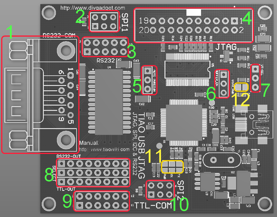
Board Layout
- DB9 male RS232 connector (Channel B)
- 2x3 standard 6 PIN 2.54mm IDC SPI connector (Channel A)
- RS232 Level 2.54mm IDC Header
- 2x10 standard 20 PIN 2.54mm IDC JTAG connector (Channel A)
- Auto power down jumper header for MAX3243 (force on or auto power down). Default force on (jumper is on pin 1and 2)
- Buffer enable jumper header for 74LVC16T245. Default is always enabled. (jumper on pin 2 and 3)
- Buffer chip 74LVC16T245 Vcc(B) power select jumper. Default is to power Vcc(B) by TUMPA (3.3V only) (jumper on pin 1 and 2)
- 3x8 PIN RS232 or TTL level serial communication jumpmer. Default is RS232 output (jumpers short top row and middle rows) (Channel B)
- 2x6 PIN TTL level 2.54mm IDC serial header (channel B)
- 2x3 PIN 2.54mm IDC SPI header (channel B)
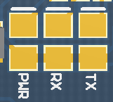
- Status LEDs. From left to right: Power (indicates TUMPA is powered on), RX and TX
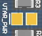
- Target board power LED. Indicates target board has power
Connector Pinout & LEDs
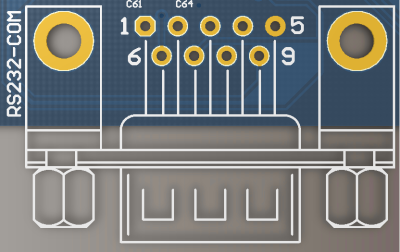
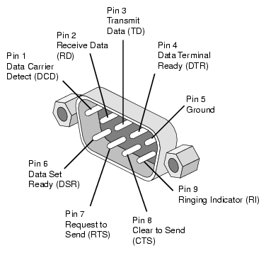
DB9 Male RS232
This connector is enabled only if RS232/TTL jumpers are on RS232-OUT, see Serial RS232/TTL level Selection Jumper
| Pin # | Acronym | Full name | Direction | Description |
|---|---|---|---|---|
| 1 | DCD | Data Carrier Detect | <<-- | Modem connected to another |
| 2 | RxD | Receive Data | <<-- | Receives bytes into PC |
| 3 | TxD | Transmit Data | -->> | Transmits bytes out of PC |
| 4 | DTR | Data Terminal Ready | -->> | I'm ready to communicate |
| 5 | SG | Signal Ground | Ground/GND | |
| 6 | DSR | Data Set Ready | <<-- | I'm ready to communicate |
| 7 | RTS | Request To Send | -->> | RTS/CTS flow control |
| 8 | CTS | Clear To Send | <<-- | RTS/CTS flow control |
| 9 | RI | Ring Indicator | <<-- | Telephone Line Ringing |
SPI Connector 1
| Pin # | Description |
|---|---|
| 1 | MISO |
| 2 | Vcc (connected to on board 3.3V) |
| 3 | SCK |
| 4 | MOSI |
| 5 | CS |
| 6 | GND |
RS232 Level 2.54mm IDC Header
This connector is enabled only if RS232/TTL jumpers are on RS232-OUT, see Serial RS232/TTL level Selection Jumper
For your convenience, we added this header. This header is inter connected to the DB9 connector. The pinout is different then the pinout of DB 9 connector, however the extra pin (PIN 10) is connected to on board 3.3V power. GND pin (PIN 9) and +3.3V PIN (PIN 10) are always enabled regardless the jumpers position of Serial RS232/TTL level Selection Jumper.
This is the pinout of the RS232 level 2.54mm IDC header:
| Pin # | Description |
|---|---|
| 1 | RI |
| 2 | DCD |
| 3 | DSR |
| 4 | CTS |
| 5 | RX |
| 6 | TX |
| 7 | RTS |
| 8 | DTR |
| 9 | GND |
| 10 | +3.3V |
20 PIN JTAG Connector
| Pin # | Description |
|---|---|
| 1 | VTAR |
| 3 | nTRST |
| 5 | TDI |
| 7 | TMS |
| 9 | TCK |
| 11 | RTCK |
| 13 | TDO |
| 15 | RST |
| 17 | DBGRQ |
| 19 | DBGACK |
| 2 | Not Connected |
| 4, 6, 8, 10, 12, 14, 16, 18, 20 | GND |
MAX3243 Auto Power Down Jumper
This jumper controls whether to always enable MAX3243 or let FT2232H automatically enables it (save power).
- Jumper on PIN 1 and PIN 2: Always enable MAX3243
- Jumper on PIN 2 and PIN 3: FT2232H (PWREN, PIN 60)controls when to enable or disable MAX3243.
Buffer Enable Jumper
This jumper controls whether to software enable/disable buffer chip (74LVC16T254).
- Jumper on PIN 1 and PIN 2: Enable (Low)/Disable (High) 74LVC16T245 via FT2232H's ACBUS3 (PIN 29).
- Jumper on PIN 2 and PIN 3: Always enable 74LVC16T245
Buffer Chip Power Selection Jumper
This jumper controls how to power the buffer / voltage translator chip (74LVC16T245)
The 74LVC16T245's Vcc(A) is connected to on board +3.3V. You can either power the Vcc(B) using on board +3.3V or powered by the target board. If powered by target board, please make sure the target board's power is in the range of +1.8V - +5.5V.
- Jumper on PIN 1 and PIN 2: Power the buffer chip 74LVC16T245's Vcc(B) via the on board +3.3V source.
- Jumper on PIN 2 and PIN 3: Power the buffer chio 74LVC16T245's Vcc(B) by target board. (PIN 3 of this header is connected to JTAG header's PIN 1)
Serial RS232/TTL level Selection Jumper
These jumpers allows you to have serial communication at either RS232 level or TTL level.
- Jumpers short top row (RS232-OUT) and middle row (SELECT) (this is the default): enable RS232 level serial output. (thus DB9 Connector and RS232 Level 2.54mm IDC Header are enabled)
- Jumpers short middle row (SELECT)and bottom row (TTL-OUT): enable TTL level serial output. (thus TTL Level Serial Connectoris enabled)
TTL Level Serial Connector
This connector is enabled only if RS232/TTL jumpers are on TTL-OUT, see Serial RS232/TTL level Selection Jumper
| Pin # | Description |
|---|---|
| 1 | Tx |
| 2 | Rx |
| 3 | RTS |
| 4 | CTS |
| 5 | DTR |
| 6 | DSR |
| 7 | DCD |
| 8 | RI |
| 9 | +3.3V |
| 10 | +5V (USB Power) |
| 11, 12 | GND |
The power pins (9, 10, 11 and 12) are always connected, regardless of the jumper positions of Serial RS232/TTL level Selection Jumper.
SPI Connector 2
| Pin # | Description |
|---|---|
| 1 | MISO |
| 2 | Vcc (connected to on board 3.3V) |
| 3 | SCK |
| 4 | MOSI |
| 5 | CS |
| 6 | GND |
PWR/RX/TX LEDs
- PWR: indicates the TUMPA board is connected to USB port of the computer and on board voltage regulator outputs +3.3V.
- RX: Indicates FT2232H is receiving bytes from target via serial communication channel B
- TX: Indicates FT2232H is transmitting bytes to target via serial communication channel B
Target Board Power LED
- LED is ON: Target board (PIN 1 of JTAG Header) has power supply > 3.3V.
- LED is OFF: Target board (PIN 1 of JTAG Header) has power supply < 3.3V or no power.
The VTAR can also be detected by software. If VTAR has voltage > 3.3V, ACBUS4 (PIN 30) of FT2232H will be LOW. Otherwise it will be HIGH.
Pin Connections
| FT2232H | 20 PIN JTAG Header | SPI Header 1 | DB9 Connector | RS232 Level Output Header | TTL Level Output Header | SPI Header 2 | Memo |
| ADBUS0 | TCK | SCK | |||||
| ADBUS1 | TDI | MOSI | |||||
| ADBUS2 | TDO | MISO | |||||
| ADBUS3 | TMS | CS | |||||
| ADBUS4 | RST | ||||||
| ADBUS5 | nTRST | ||||||
| ADBUS6 | DBGRQ | ||||||
| ADBUS7 | RTCK | ||||||
| ACBUS0 | DBGACK | ||||||
| ACBUS1 | Connected to nTRST pin of JTAG Header, (input) | ||||||
| ACBUS2 | Connected to RST pin of JTAG Header, as (input) | ||||||
| ACBUS3 | OEN Pin (enable buffer chip), active low (output) | ||||||
| ACBUS4 | Target present pin. Detect VTAR, active low (input) | ||||||
| ACBUS5 | |||||||
| ACBUS6 | |||||||
| ACBUS7 | |||||||
| BDBUS0 | TX | TX | TX | SCK | |||
| BDBUS1 | RX | RX | RX | MOSI | |||
| BDBUS2 | RTS | RTS | RTS | MISO | |||
| BDBUS3 | CTS | CTS | CTS | CS | |||
| BDBUS4 | DTR | DTR | DTR | ||||
| BDBUS5 | DSR | DSR | DSR | ||||
| BDBUS6 | DCD | DCD | DCD | ||||
| BDBUS7 | RI | RI | RI | ||||
| BCBUS0 | |||||||
| BCBUS1 | |||||||
| BCBUS2 | |||||||
| BCBUS3 | RX LED | ||||||
| BCBUS4 | TX LED | ||||||
| BCBUS5 | |||||||
| BCBUS6 | |||||||
| BCBUS7 | |||||||
| PWREN | Enable MAX3243. Active low (output) |
Buy various JTAG cables for your Satellite Receiver, Cable Modem, Wireless Router, Standard Wiggler from http://www.easymg.com and http://www.diygadget.com

10 PCS, 10cm x 10cm, 2 layers prototype for $38.80 shipped!
