Difference between revisions of "TIAO USB Multi Protocol Adapter Lite User's Manual"

10 PCS, 10cm x 10cm, 2 layers prototype for $38.80 shipped!
(→20 PIN JTAG Connector) |
|||
| Line 204: | Line 204: | ||
| GND | | GND | ||
|} | |} | ||
| + | |||
| + | |||
| + | == GPIO Header 1 == | ||
| + | |||
| + | These pins are either power pins or directly connected to GPIO pins of FT232H. | ||
| + | |||
| + | {| | ||
| + | ! align="left"|Pin # | ||
| + | ! Description | ||
| + | |- | ||
| + | | 1, 2 | ||
| + | | GND | ||
| + | |- | ||
| + | | 3, 4 | ||
| + | | +3.3V of TUMPA Lite's onboard LDO output. | ||
| + | |- | ||
| + | | 5, 6 | ||
| + | | +5V output (From USB power) | ||
| + | |- | ||
| + | | 7, 8 | ||
| + | | ''REST#'' | ||
| + | |- | ||
| + | | 9, 10 | ||
| + | | ''AC9'' | ||
| + | |- | ||
| + | | 11, 12 | ||
| + | | ''AC8'' | ||
| + | |- | ||
| + | | 13, 14 | ||
| + | | ''AC7'' | ||
| + | |- | ||
| + | | 15, 16 | ||
| + | | ''AC6'' | ||
| + | |- | ||
| + | | 17, 18 | ||
| + | | ''AC5'' | ||
| + | |- | ||
| + | | 19, 20 | ||
| + | | ''AC4'' | ||
| + | |- | ||
| + | | 21, 22 | ||
| + | | ''AC3'' | ||
| + | |- | ||
| + | | 23, 24 | ||
| + | | ''AC2'' | ||
| + | |- | ||
| + | | 25, 26 | ||
| + | | ''AC1'' | ||
| + | |- | ||
| + | | 27, 28 | ||
| + | | ''AC0'' | ||
| + | |} | ||
| + | |||
| + | |||
| + | |||
| + | |||
== DB9 Male RS232 == | == DB9 Male RS232 == | ||
Revision as of 15:03, 6 October 2012
Contents
- 1 Overview
- 2 Technical Specifications
- 3 Board Dimensions
- 4 Board Layout
- 5 Connector Pinout & LEDs
- 5.1 RX TX LED Config Header
- 5.2 SPI Connector
- 5.3 SPI MISO Pullup Config Header
- 5.4 20 PIN JTAG Connector
- 5.5 GPIO Header 1
- 5.6 DB9 Male RS232
- 5.7 SPI Connector 1
- 5.8 RS232 Level 2.54mm IDC Header
- 5.9 20 PIN JTAG Connector
- 5.10 MAX3243 Auto Power Down Jumper
- 5.11 Buffer Enable Jumper
- 5.12 Buffer Chip Power Selection Jumper
- 5.13 Serial RS232/TTL level Selection Jumper
- 5.14 TTL Level Serial Connector
- 5.15 SPI Connector 2
- 5.16 PWR/RX/TX LEDs
- 5.17 Target Board Power LED
- 6 Pin Connections
Buy various JTAG cables for your Satellite Receiver, Cable Modem, Wireless Router, Standard Wiggler from http://www.easymg.com and http://www.diygadget.com
Overview
The TIAO USB Multi Protocol Adapter Lite (TUMPA Lite) is a multi-functional USB communication adapter for hobbyists or engineers. The adapter is based on FDTI's flagship communication chip FT232H, a USB 2.0 Hi-Speed (480Mb/s) to UART/FIFO IC. It has one multi-protocol synchronous serial engines (MPSSEs) which allow for communication using JTAG, I2C and SPI on two channels simultaneously.
Technical Specifications
- Single channel USB to serial / parallel ports with a variety of configurations.
- Entire USB protocol handled on the chip. No USB specific firmware programming required.
- USB 2.0 Hi-Speed (480Mbits/Second) and Full Speed (12Mbits/Second) compatible.
- Multi-Protocol Synchronous Serial Engine (MPSSE) to simplify synchronous serial protocol (USB to JTAG, I2C, SPI or bit-bang) design.
- UART transfer data rate up to 12Mbaud. (RS232 Data Rate limited by external level shifter).
- USB to asynchronous 245 FIFO mode for transfer data rate up to 8 MByte/Sec.
- USB to synchronous 245 parallel FIFO mode for transfers up to 40 Mbytes/Sec
- Supports a half duplex FT1248 interface with a configurable width, bi-directional data bus (1, 2, 4 or 8 bits wide).
- CPU-style FIFO interface mode simplifies CPU interface design.
- Fast serial interface option.
- FTDI's royalty-free Virtual Com Port (VCP) and Direct (D2XX) drivers eliminate the requirement for USB driver development in most cases.
- Adjustable receive buffer timeout.
- Option for transmit and receive LED drive signals.
- Bit-bang Mode interface option with RD# and WR strobes
- Highly integrated design includes 5V to 3.3/+1.8V LDO regulator for VCORE, integrated POR function
- Asynchronous serial UART interface option with full hardware handshaking and modem interface signals.
- Fully assisted hardware or X-On / X-Off software handshaking.
- UART Interface supports 7/8 bit data, 1/2 stop bits, and Odd/Even/Mark/Space/No Parity.
- Auto-transmit enable control for RS485 serial applications using TXDEN pin.
- Operation configuration mode and USB Description strings configurable in external EEPROM over the USB interface.
- Configurable I/O drives strength (4, 8, 12 or 16mA) and slew rate.
- Low operating and USB suspend current.
- Supports self powered, bus powered and high-power bus powered USB configurations.
- UHCI/OHCI/EHCI host controller compatible.#
- USB Bulk data transfer mode (512 byte packets in Hi-Speed mode).
- +1.8V (chip core) and +3.3V I/O interfacing (+5V Tolerant).
- Extended -40°C to 85°C industrial operating temperature range.
- Compact 48-pin Lead Free LQFP or QFN package
- Configurable ACBUS I/O pins.
- 4 on-board LEDs / PWR, +3.3V Out, TX and RX
- 1 2x10 20 PIN JTAG header
- 1 2x3 6 PIN SPI 2.54mm IDC header
- 1 SPI MISO pullup config IDC header
- 1 Configurable TX/RX LED IDC header
- On board 3.3V LDO
- USB over-current protection via on-board resetable fuse.
- Strong ESD protection on USB signals.
- Based on the FTDI FT232H USB device.
- Designed for FTDI MPSSE easy-to-use.
- Free drivers for Linux.
- Free drivers for Windows XP, Windows Vista and Windows 7
- Support both 32 bit and 64 bit operating systems
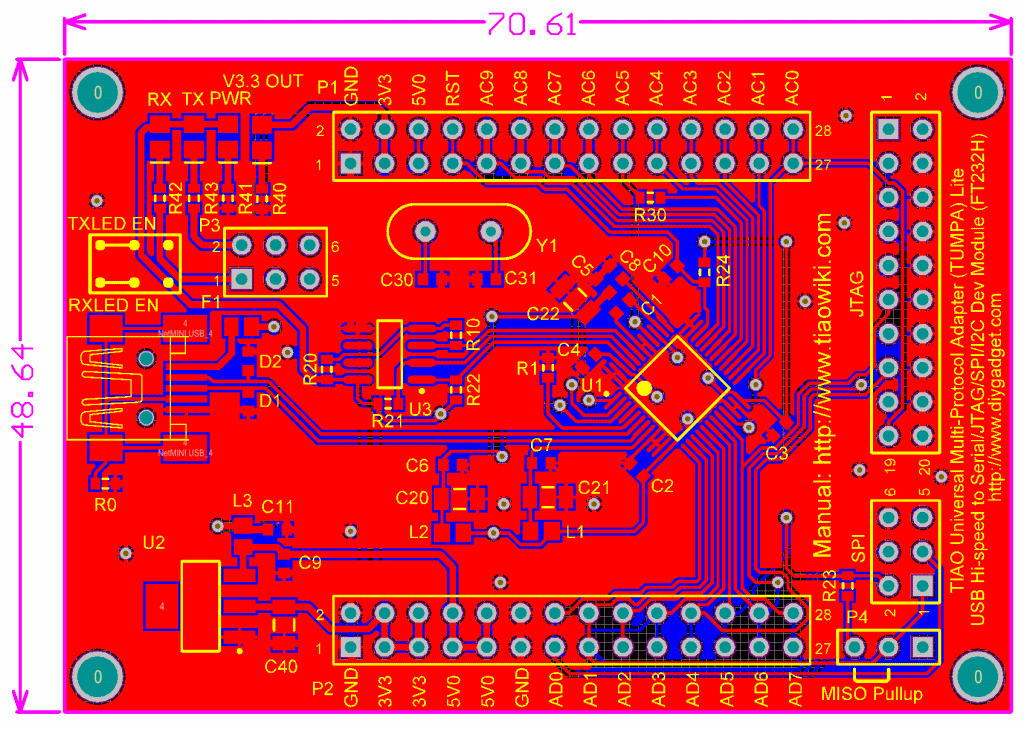
- Board dimension: 48.64mm X 70.61mm (1.91" X 2.78")
Board Dimensions
Board Layout
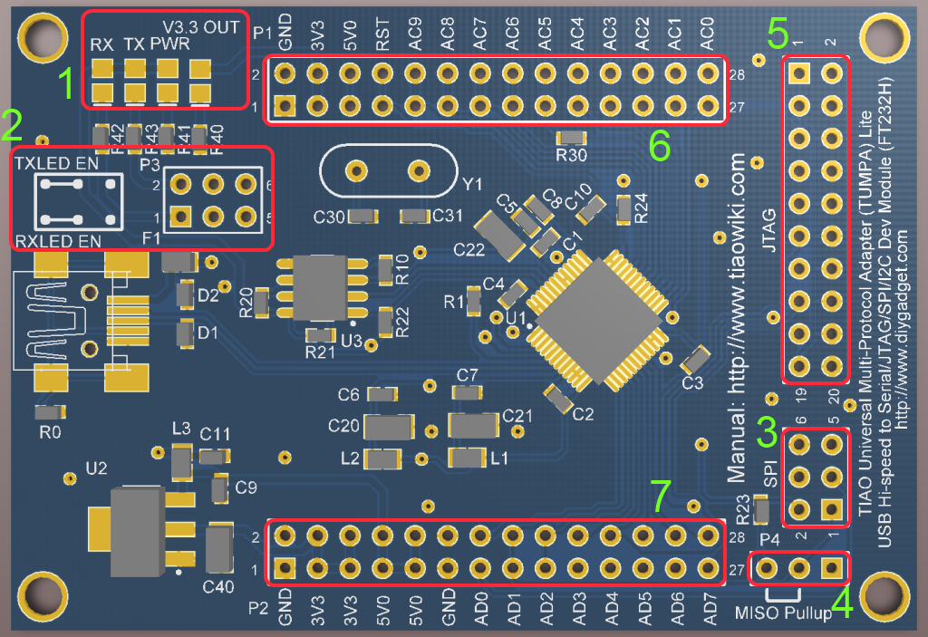
- LEDs - RX/TX/PWR/+3.3V Output
- 2x3 standard 6 PIN 2.54mm IDC for RX/TX LED
- 2x3 PIN 2.54mm IDC SPI header
- SPI MISO pullup enable header
- 2x10 standard 20 PIN 2.54mm IDC JTAG connector
- 2x14 PIN 2.54mm IDC GPIO Pins
- 2x14 PIN 2.54mm IDC GPIO Pins
Connector Pinout & LEDs
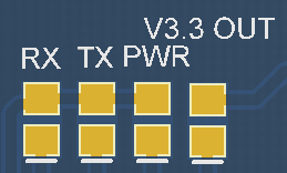
- RX: Indicates FT232H is receiving bytes from target via serial communication channel. See 2x3 standard 6 PIN 2.54mm IDC for RX/TX LED on how to enable this.
- TX: Indicates FT232H is transmitting bytes to target via serial communication channel. See 2x3 standard 6 PIN 2.54mm IDC for RX/TX LED on how to enable this.
- PWR: Indicates the TUMPA Lite board is connected to USB port of the computer and FT232H's onboard voltage regulator outputs +3.3V.
- V3.3 Out: Indicates the TUMPA Lite's onboard voltage LDO outputs +3.3V.
RX TX LED Config Header
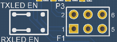
This jumper header enables LED output on RX and TX.
With FT232H's default configuration, AC8 is the RX led output pin, AC9 is the TX led output pin.
Install a jumper on pin 1 and 3 enables RX LED. Install a jumper on pin 2 and 4 enables TX LED.
If AC8 and AC9 are configured for GPIO, you need to remove jumpers on this header.
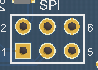
SPI Connector
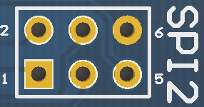
| Pin # | Description |
|---|---|
| 1 | MISO |
| 2 | Vcc (connected to on board 3.3V) |
| 3 | SCK |
| 4 | MOSI |
| 5 | CS |
| 6 | GND |
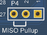
SPI MISO Pullup Config Header
Install a jumper on pin 2 and 3 to enable MISO pullup resistor (10K) to
20 PIN JTAG Connector
| Pin # | FT232H Pin | Description |
|---|---|---|
| 1 | Not Connected | Not Connected |
| 3 | AD5 | nTRST |
| 5 | AD1 | TDI |
| 7 | AD3 | TMS |
| 9 | AD0 | TCK |
| 11 | AD7 | RTCK |
| 13 | AD2 | TDO |
| 15 | AD4 | RST |
| 17 | AD6 | DBGRQ |
| 19 | AC0 | DBGACK |
| 2 | Not Connected | Not Connected |
| 4, 6, 8, 10, 12, 14, 16, 18, 20 | GND | GND |
GPIO Header 1
These pins are either power pins or directly connected to GPIO pins of FT232H.
| Pin # | Description |
|---|---|
| 1, 2 | GND |
| 3, 4 | +3.3V of TUMPA Lite's onboard LDO output. |
| 5, 6 | +5V output (From USB power) |
| 7, 8 | REST# |
| 9, 10 | AC9 |
| 11, 12 | AC8 |
| 13, 14 | AC7 |
| 15, 16 | AC6 |
| 17, 18 | AC5 |
| 19, 20 | AC4 |
| 21, 22 | AC3 |
| 23, 24 | AC2 |
| 25, 26 | AC1 |
| 27, 28 | AC0 |
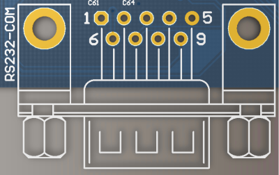
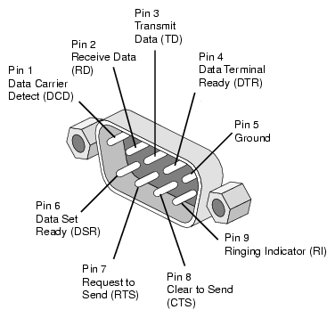
DB9 Male RS232
This connector is enabled only if RS232/TTL jumpers are on RS232-OUT, see Serial RS232/TTL level Selection Jumper
| Pin # | Acronym | Full name | Direction | Description |
|---|---|---|---|---|
| 1 | DCD | Data Carrier Detect | <<-- | Modem connected to another |
| 2 | RxD | Receive Data | <<-- | Receives bytes into PC |
| 3 | TxD | Transmit Data | -->> | Transmits bytes out of PC |
| 4 | DTR | Data Terminal Ready | -->> | I'm ready to communicate |
| 5 | SG | Signal Ground | Ground/GND | |
| 6 | DSR | Data Set Ready | <<-- | I'm ready to communicate |
| 7 | RTS | Request To Send | -->> | RTS/CTS flow control |
| 8 | CTS | Clear To Send | <<-- | RTS/CTS flow control |
| 9 | RI | Ring Indicator | <<-- | Telephone Line Ringing |
SPI Connector 1
| Pin # | Description |
|---|---|
| 1 | MISO |
| 2 | Vcc (connected to on board 3.3V) |
| 3 | SCK |
| 4 | MOSI |
| 5 | CS |
| 6 | GND |
RS232 Level 2.54mm IDC Header
This connector is enabled only if RS232/TTL jumpers are on RS232-OUT, see Serial RS232/TTL level Selection Jumper
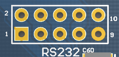
For your convenience, we added this header. This header is inter connected to the DB9 connector. The pinout is different then the pinout of DB 9 connector, however the extra pin (PIN 10) is connected to on board 3.3V power. GND pin (PIN 9) and +3.3V PIN (PIN 10) are always enabled regardless the jumpers position of Serial RS232/TTL level Selection Jumper.
This is the pinout of the RS232 level 2.54mm IDC header:
| Pin # | Description |
|---|---|
| 1 | RI |
| 2 | DCD |
| 3 | DSR |
| 4 | CTS |
| 5 | RX |
| 6 | TX |
| 7 | RTS |
| 8 | DTR |
| 9 | GND |
| 10 | +3.3V |
20 PIN JTAG Connector
| Pin # | Description |
|---|---|
| 1 | VTAR |
| 3 | nTRST |
| 5 | TDI |
| 7 | TMS |
| 9 | TCK |
| 11 | RTCK |
| 13 | TDO |
| 15 | RST |
| 17 | DBGRQ |
| 19 | DBGACK |
| 2 | Not Connected |
| 4, 6, 8, 10, 12, 14, 16, 18, 20 | GND |
MAX3243 Auto Power Down Jumper
This jumper controls whether to always enable MAX3243 or let FT2232H automatically enables it (save power).
- Jumper on PIN 1 and PIN 2: Always enable MAX3243
- Jumper on PIN 2 and PIN 3: FT2232H (PWREN, PIN 60)controls when to enable or disable MAX3243.
Buffer Enable Jumper
This jumper controls whether to software enable/disable buffer chip (74LVC16T254).
- Jumper on PIN 1 and PIN 2: Enable (Low)/Disable (High) 74LVC16T245 via FT2232H's ACBUS3 (PIN 29).
- Jumper on PIN 2 and PIN 3: Always enable 74LVC16T245
Buffer Chip Power Selection Jumper
This jumper controls how to power the buffer / voltage translator chip (74LVC16T245)
The 74LVC16T245's Vcc(A) is connected to on board +3.3V. You can either power the Vcc(B) using on board +3.3V or powered by the target board. If powered by target board, please make sure the target board's power is in the range of +1.8V - +5.5V.
- Jumper on PIN 1 and PIN 2: Power the buffer chip 74LVC16T245's Vcc(B) via the on board +3.3V source.
- Jumper on PIN 2 and PIN 3: Power the buffer chio 74LVC16T245's Vcc(B) by target board. (PIN 3 of this header is connected to JTAG header's PIN 1)
Serial RS232/TTL level Selection Jumper
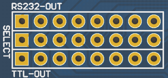
These jumpers allows you to have serial communication at either RS232 level or TTL level.
- Jumpers short top row (RS232-OUT) and middle row (SELECT) (this is the default): enable RS232 level serial output. (thus DB9 Connector and RS232 Level 2.54mm IDC Header are enabled)
- Jumpers short middle row (SELECT)and bottom row (TTL-OUT): enable TTL level serial output. (thus TTL Level Serial Connectoris enabled)
TTL Level Serial Connector
This connector is enabled only if RS232/TTL jumpers are on TTL-OUT, see Serial RS232/TTL level Selection Jumper
| Pin # | Description |
|---|---|
| 1 | Tx |
| 2 | Rx |
| 3 | RTS |
| 4 | CTS |
| 5 | DTR |
| 6 | DSR |
| 7 | DCD |
| 8 | RI |
| 9 | +3.3V |
| 10 | +5V (USB Power) |
| 11, 12 | GND |
The power pins (9, 10, 11 and 12) are always connected, regardless of the jumper positions of Serial RS232/TTL level Selection Jumper.
SPI Connector 2
| Pin # | Description |
|---|---|
| 1 | MISO |
| 2 | Vcc (connected to on board 3.3V) |
| 3 | SCK |
| 4 | MOSI |
| 5 | CS |
| 6 | GND |
PWR/RX/TX LEDs
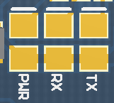
- PWR: indicates the TUMPA board is connected to USB port of the computer and on board voltage regulator outputs +3.3V.
- RX: Indicates FT2232H is receiving bytes from target via serial communication channel B
- TX: Indicates FT2232H is transmitting bytes to target via serial communication channel B
Target Board Power LED
- LED is ON: Target board (PIN 1 of JTAG Header) has power supply > 3.3V.
- LED is OFF: Target board (PIN 1 of JTAG Header) has power supply < 3.3V or no power.
The VTAR can also be detected by software. If VTAR has voltage > 3.3V, ACBUS4 (PIN 30) of FT2232H will be LOW. Otherwise it will be HIGH.
Pin Connections
| FT2232H | 20 PIN JTAG Header | SPI Header 1 | DB9 Connector | RS232 Level Output Header | TTL Level Output Header | SPI Header 2 | Memo |
| ADBUS0 | TCK | SCK | |||||
| ADBUS1 | TDI | MOSI | |||||
| ADBUS2 | TDO | MISO | |||||
| ADBUS3 | TMS | CS | |||||
| ADBUS4 | RST | ||||||
| ADBUS5 | nTRST | ||||||
| ADBUS6 | DBGRQ | ||||||
| ADBUS7 | RTCK | ||||||
| ACBUS0 | DBGACK | ||||||
| ACBUS1 | Connected to nTRST pin of JTAG Header, (input) | ||||||
| ACBUS2 | Connected to RST pin of JTAG Header, as (input) | ||||||
| ACBUS3 | OEN Pin (enable buffer chip), active low (output) | ||||||
| ACBUS4 | Target present pin. Detect VTAR, active low (input) | ||||||
| ACBUS5 | |||||||
| ACBUS6 | |||||||
| ACBUS7 | |||||||
| BDBUS0 | TX | TX | TX | SCK | |||
| BDBUS1 | RX | RX | RX | MOSI | |||
| BDBUS2 | RTS | RTS | RTS | MISO | |||
| BDBUS3 | CTS | CTS | CTS | CS | |||
| BDBUS4 | DTR | DTR | DTR | ||||
| BDBUS5 | DSR | DSR | DSR | ||||
| BDBUS6 | DCD | DCD | DCD | ||||
| BDBUS7 | RI | RI | RI | ||||
| BCBUS0 | |||||||
| BCBUS1 | |||||||
| BCBUS2 | |||||||
| BCBUS3 | RX LED | ||||||
| BCBUS4 | TX LED | ||||||
| BCBUS5 | |||||||
| BCBUS6 | |||||||
| BCBUS7 | |||||||
| PWREN | Enable MAX3243. Active low (output) |
Buy various JTAG cables for your Satellite Receiver, Cable Modem, Wireless Router, Standard Wiggler from http://www.easymg.com and http://www.diygadget.com

10 PCS, 10cm x 10cm, 2 layers prototype for $38.80 shipped!
